SoCCanvasSecondDemo – Clock Diagram
Clock은 신호가 아니라 시스템 구조입니다.
🧭 How to design SoC with SoC Canvas
Episode 2에서는
GUI로 Clock 구조를 직접 설계하는 과정을 보여드립니다.
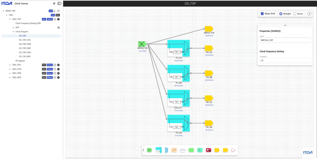
PLL, MUX, Divider, Gate등을 자유롭게 조합하여
복잡한 Clock구조를 손쉽게 설계할 수 있습니다.
Canvas GUI에 그린 Clock Diagram이 곧 Hardware로 생성되며
모든 Clock Node들의 주파수와 각 Component들의 설정 값을 한눈에 확인할 수 있고
해당 정보가 모든 설계 결과물에 그대로 반영되어 생성됩니다.
이번 영상에서는
Clock Diagram을 통해 구조를 설계하는 과정을 확인하실 수 있습니다.
🎥 Episode 2: Clock Diagram
▶️ 전체 데모 영상이 궁금하신 분들은 댓글이나 DM 주시면 링크를 공유해드리겠습니다.
SoCCanvasSecondDemo – Clock Diagram
A clock is not a signal, but a system structure.
🧭How to design SoC with SoC Canvas
In Episode 2,
we demonstrate the process of directly designing a clock structure using the GUI.
You can easily design complex clock structures
by freely combining PLLs, MUXs, dividers, gates, and more.
The clock diagram drawn on the Canvas GUI is immediately generated as hardware
you can view the frequencies of all clock nodes and the settings of each component at a glance,
and this information is directly reflected in all design results.
In this video,you can see the process of designing a structure using a clock diagram.
🎥 Episode 2: Clock Diagram
▶️ If you are interested in the full demo video, please leave a comment or send a DM, and we will share the link.
💡 Summary
In this video, we explore the Clock Diagram feature in SoC Canvas.
Instead of treating clocks as static parameters,
we model them as a structured system of PLLs, MUXes, and dividers.
With a visual graph-based approach,
you can design, modify, and manage the clock architecture intuitively.
As changes are made,
SFRs (Special Function Registers) are automatically generated
and kept in sync in real time.
📌 Key moments:
00:00 – Understanding Clock System Structures
00:21 – Defining Clock Sources & Roots
00:41 – Visual Design: Designing Clock Diagrams Freely
01:03 – Exploring Clock Components (PLL, MUX, Divider, Gates)
01:25 – Automatic SFR Generation & Mapping
01:48 – Real-time Component Configuration & Sync
02:32 – Finalizing the CMU (Clock Management Unit) Design