So far, we have looked at the problems of the Clock system and Power system, which are the infrastructures that are intertwined with the DFT system and make DFT configuration difficult.
Now, we need to test the Hard IP.
Since the Hard IP, which is usually provided as a black box, has an unknown internal structure, the DFT is configured based on the test wrapper provided by the IP supplier. This wrapper provides a minimum test interface that can access the inside of the Hard IP, and although it looks simple, it is not easy.
What is the biggest limitation that makes it difficult to connect to the wrapper for testing the Hard IP?
It is that the number of I/O that the designer can control is too small.
Usually, the number of GPIOs in the entire SoC is around 100. This means that even if you use all the GPIOs for testing, there are still about 100 I/O pins. However, these days, high-performance IPs such as PCIe 5.0 have over 1,000 pins, and SoCs do not only have PCIe. Many types of IPs such as ADC, USB, DDR PHY, and temperature sensors are included. All the pins inside the SoC are subjects of test, so in the end, thousands of pins need to be tested with about 100 I/O.
Here, the designer’s only options are a MUX/DEMUX configuration or a BUS configuration.
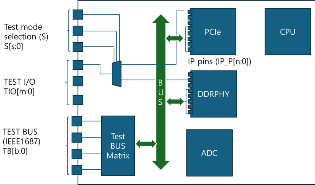
Looking at the MUX/DEMUX configuration in the simplified diagram above,
first, there must be a selection signal, S[s:0], which determines which IP to send a signal to. If you decide to test PCIe with this signal, the GPIO pins are mapped 1:1 with the PCIe pins and tested. But s has a maximum of 100 GPIO pins, but the number n of PCIe pins (IP_P[n:0]) exceeds 1000, so 1:1 mapping is not possible. Testing is not possible. The same goes for DEMUX. Therefore, the problem of insufficient Input I/O cannot be solved with the MUX/DEMUX form.
However, not all signals can be implemented in the form of a BUS. This is because signals that must be mapped 1:1 with I/O, such as the Clock signal (TIO[m:0]), can only be implemented in the form of a MUX/DEMUX.
In other words, even if the MUX form is used, it can only be configured in a form that is mixed with the BUS. In order to implement the DFT of the hard IP, due to the insufficient I/O, an ambiguous form of configuration that mixes the BUS and MUX/DEMUX forms is the best.
Fortunately, this form of configuration itself is not difficult. However, the problem is the complexity that I have mentioned many times. There are too many numbers to configure. Moreover, this complexity is always a bigger problem because it occurs at the last stage of the design.
Let’s take an example of this complexity. Let’s say there is a SoC with 100 GPIOs. Let’s assume that there are 30 hard IPs in this SoC, and each hard IP has 200 pins to control. So, 30 x 200 = 6,000 pins in total have to be controlled. In this case, one GPIO has to control more than 60 pins on average. You have to define and map exactly which IP and pin each of the 60 signals coming into each of the 100 GPIOs should be connected to. The bigger problem is that this definition and mapping always has to be done at the last stage of the chip design, that is, at the DFT insertion stage after implementation. Checking this at the last stage increases the possibility of a design error.
Then, can you proceed with the DFT configuration at the RTL stage, which is the beginning of the design? Even if you do this, verification becomes a problem. Hard IP tests are vector-based, but SoCs are verification-based, so vectors need to be converted to a verification level that SoCs can understand, and this needs to be verified in advance. This is not easy either.
We need a different method.
지금까지 DFT 시스템과 얽혀 DFT 구성을 어렵게 하는 인프라인 Clock 시스템과 Power 시스템의 문제에 대해 살펴봤습니다.
이제 Hard IP를 테스트 해야 합니다.
보통 블랙박스로 제공되는 Hard IP는 내부 구조를 알 수 없기 때문에, IP 공급 업체가 제공하는 테스트 wrapper를 기반으로 DFT를 구성하게 됩니다. 이 wrapper는 Hard IP 내부에 접근 할 수 있는 최소한의 테스트 인터페이스를 제공하는데, 보기에는 간단한 것 같지만, 쉽지 않습니다.
Hard IP를 테스트하기 위한 wrapper와의 연결을 어렵게 하는 가장 큰 제약 사항은 무엇일까요?
바로 설계자가 제어할 수 있는 I/O의 개수가 너무 부족하다는 점입니다.
보통 SoC 전체의 GPIO는 100개 안팎입니다. 테스트를 위해 모든 GPIO를 다 써도 I/O 핀이 100개 정도라는 얘기입니다. 그런데, 요즘 PCIe 5.0 같은 고성능 IP는 핀이 1000개가 넘는데, SoC에는 PCIe만 있는게 아니죠. ADC, USB, DDR PHY, 온도 센서등 수많은 종류의 IP들이 들어갑니다. SoC 내부의 핀들은 다 테스트 대상이라, 결국 100개정도의 I/O로 수천 개의 핀들을 테스트 해야 한다는 얘기입니다.
여기서 설계자의 선택지는 MUX/DEMUX 형태 구성 혹은 BUS 형태의 구성 뿐입니다.
위의 간략화한 그림으로 MUX/DEMUX 형태의 구성을 살펴보면,
먼저 어떤 IP에 신호를 전달할 지를 결정하는 selection 신호, S[s:0]가 있어야 합니다. 이 신호로 PCIe를 테스트 하기로 정하면, GPIO 핀들이 PCIe의 핀들과 1:1로 mapping이 되어 테스트를 하게 됩니다. 그런데 s는 GPIO 핀의 최대치가 100개 안팎인데, PCIe의 핀 (IP_P[n:0])의 갯수 n은 최대치가 1000개가 넘는 상황이라 1:1 mapping이 안됩니다. 테스트를 할 수가 없습니다. DEMUX의 경우도 마찬가지입니다. 따라서 Input I/O가 부족한 문제는 MUX/DEMUX 형태로는 해결할 수 없습니다.
그렇다고 모든 신호를 BUS의 형태로 구현할 수도 없습니다. 왜냐하면, Clock 신호의 경우처럼 I/O와 1:1로 mapping되어야 하는 신호(TIO[m:0])의 경우는 MUX/DEMUX 형태로 구현할 수 밖에 없기 때문입니다.
즉, MUX형태를 사용해도, BUS 와 혼합되는 형태의 구성을 할 수 밖에 없는 것이죠. Hard IP의 DFT 구현을 위해서는, 부족한 I/O로 인해, BUS와 MUX/DEMUX 형태를 섞어서 사용하는 애매한 형태의 구성이 최선이라는 얘기입니다.
다행히도 이러한 형태의 구성 자체는 어렵지 않습니다. 다만, 문제는 여러 번 얘기했던 복잡도 입니다. 구성 해야 할 숫자가 너무 많습니다. 거기다 이러한 복잡도는 항상 설계의 마지막 단계에서 발생하게 되는 것이 더 큰 문제입니다.
이 복잡도에 대한 를 들어 보겠습니다. GPIO가 100개인 SoC가 있습니다. 이 SoC에는 30개의 Hard IP가 들어가고, 각 Hard IP 당 제어해야 할 핀이 200개씩이라고 가정하면,
30×200=6,000 총 6천개의 핀을 제어해야 합니다. 이 경우엔 하나의 GPIO가 평균 60개 이상의 핀을 제어해야 하죠. 100개의 GPIO 하나하나에 들어오는 60개의 신호들을 어떤 IP, 어떤 핀과 연결되어야 하는 지를 정확히 정의하고 mapping해야합니다. 더 큰 문제는 이 정의와 mapping이 언제나 칩의 설계 마지막 단계, 즉 implementation이후의 DFT insertion단계에서 해야 한다는 것입니다. 이것을 마지막 단계에서 확인하는 것은 설계가 잘못될 가능성을 높이게 되는 것입니다.
그럼 DFT 구성을 설계의 시작인 RTL 단계에서 진행하면 될까요? 이렇게 해도 검증이 문제가 됩니다. Hard IP는 테스트는 벡터 위주로 동작하는데, SoC는 verification위주로 동작하기 때문에 vector를 SoC가 이해할 수 있는 verification level로 변환하고, 이를 미리 검증할 수 있도록 해줘야 합니다. 이것도 쉽지 않습니다.
우리에게는 좀 더 다른 방법이 필요합니다.