In semiconductor design, SoC design involves a stage called Integration.
In contrast, in MCU or analog-focused chip design, this process is naturally embedded in the design flow
and is often not recognized as a separate stage.
As a result, the concept of Integration may be absent or felt very weakly.
So why did Integration emerge and what does it involve?
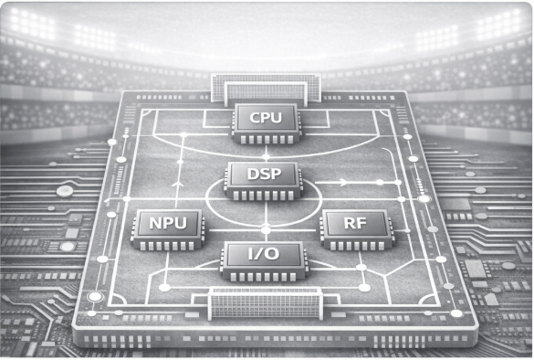
In SoC design, Integration refers to the process of assembling individually designed IPs
into a single system that operates according to the intended design.
It is not simply connecting IPs with wiring.
It is the entire process of ensuring that each IP works together in a single chip
under the same clock, reset philosophy, and power and security structure.
We call this process Integration, not Combination.
The result of Integration cannot be a system that only partially works or a chip that operates conditionally.
It is the process of making the entire chip operate consistently within the same design intention
for clocks, resets, power, and interfaces.
No matter how perfect each IP is individually,
if they cannot be properly integrated into a single system, the chip cannot exist.
Thus, Integration in SoC is not just a final step but the last design stage required to make the chip a functional chip.
When the chip is small, this process is naturally embedded in the design flow.
There are few resets, the clock structure is simple, and IP and system boundaries are not clearly separated.
To put it simply,
building a few houses in a rural village is like constructing the roads, electricity, and water supply while building the houses.
However, if you are developing a new city, this method is not sufficient to create a proper city.
As chips become larger, more complex, and IP-based design becomes common,
Integration becomes an independent and important design area.
Integration in SoC is often thought of as connecting components.
Indeed, many tools provide connection-focused functionality,
and much of the work on site is spent on wiring, which is why it may seem that way.
However, the essence of SoC Integration is not simple connection.
It is the process of concretizing the design intention embedded in the system
such as clocks, resets, bus structures, security, and power,
through decisions about which line to connect and why.
In this way, SoC Integration is a very unique form of design
where system design, roles and responsibilities, and design methodology meet at a single point.
반도체 설계를 하다 보면, SoC 설계에서는 Integration이라는 단계가 존재합니다.
반면 MCU나 아날로그 중심의 칩 설계에서는, 이 과정이 설계 흐름 안에 자연스럽게 녹아 있어, 독립된 단계로 인식되지 않는 경우가 많았습니다.
그래서 Integration이라는 개념 자체가 없거나, 매우 약하게 느껴지기도 합니다.
그렇다면 Integration은 왜 등장했고, 무엇을 하는 단계일까요?
SoC 설계에서 Integration이란,
개별적으로 설계된 IP들을 모아서 하나의 시스템으로 의도대로 동작하도록 구성하는 과정을 의미합니다.
단순히 IP들을 나열해 wiring으로 연결하는 것이 아니라,
각 IP가 같은 클록, 같은 리셋 철학, 같은 전력·보안 구조 안에서
하나의 칩으로 동작하도록 만드는 전 과정이 Integration입니다.
이 과정을 우리는 ‘조합(Combination)’이 아니라 ‘통합(Integration)’이라고 부릅니다.
Integration의 결과물은 일부만 맞는 시스템이나 조건부로만 동작하는 칩이 될 수 없습니다.
클록, 리셋, 전력, 인터페이스가 모두 같은 설계 의도 안에서
칩 전체가 일관되게 동작하도록 만드는 것,
그 과정이 바로 Integration입니다.
아무리 각 IP가 개별적으로 완벽하더라도,
이를 하나의 시스템으로 제대로 녹여내지 못하면 칩이 되지 못합니다.
그래서 SoC에서 integration은 단순한 마무리 작업이 아니라,
칩이 칩이 되기 위한 마지막 설계 단계라고 볼 수 있습니다.
칩의 규모가 작을 때는 이 과정이 자연스럽게 설계 흐름 안에 녹아 있습니다.
리셋은 몇 개 되지 않고, 클록 구조도 단순하며, IP와 시스템이 명확히 분리되지 않기 때문입니다.
간단하게 비유 하자면,
집이 몇채 있는 시골 마을에서는 집을 지으면서 도로나 전기, 수도 공사를 함께 진행하는 것과 비슷합니다.
하지만, 신도시를 개발한다면, 이런 방식으로는 정상적으로 도시를 만들 수 없습니다.
칩이 커지고, 기능이 복잡해지고, IP 단위 설계가 일반화되면서,
Integration은 하나의 독립적이고 중요한 설계 영역으로 자리 잡게 되었습니다.
흔히 SoC Integration을 연결하는 일이라고 생각합니다.
실제로 많은 툴들이 연결 중심의 기능을 제공하고,
현장에서의 작업량 대부분도 wiring에 쓰이기 때문에 그렇게 보이기도 합니다.
하지만 SoC Integration의 본질은 단순한 연결이 아닙니다.
그것은 클록, 리셋, 버스 구조, 보안, 파워처럼 시스템 전반에 담긴 설계 의도를
어떤 선을, 왜 그곳에 연결할 것인가라는 선택을 통해 하나씩 구체화 해가는 과정입니다.
이렇게 보면 SoC Integration은
시스템 설계, 역할과 책임(R&R), 그리고 설계 방법론이 한 지점에서 만나는
매우 독특한 형태의 설계 과정이라고 할 수 있습니다.