Why did we choose to make our product a GUI?
GUI stands for Graphic User Interface, a system that allows users to interact with a product through visual elements.
Put differently, it’s a way of communicating through pictures.
Language and text are also forms of communication, but they must be learned and interpreted. Pictures, however, are different.
They are intuitively understandable without prior learning.
Because what you see is represented directly, people from different languages and cultures can grasp the meaning immediately.
Moreover, simple actions like clicking or scrolling allow users to execute their intentions right away.
GUI is the most natural and intuitive way to communicate, aligned with human perception and thought processes.
This is why, after GUI was applied to the Macintosh, computers were no longer tools only for experts who knew Fortran or C.
They became tools that anyone could use in everyday life.
We applied the same philosophy to our product.
We made it a GUI to directly express the thoughts of semiconductor engineers and make design easier.
Semiconductor design is coded in Verilog or C, but most designers don’t actually understand semiconductors through code.
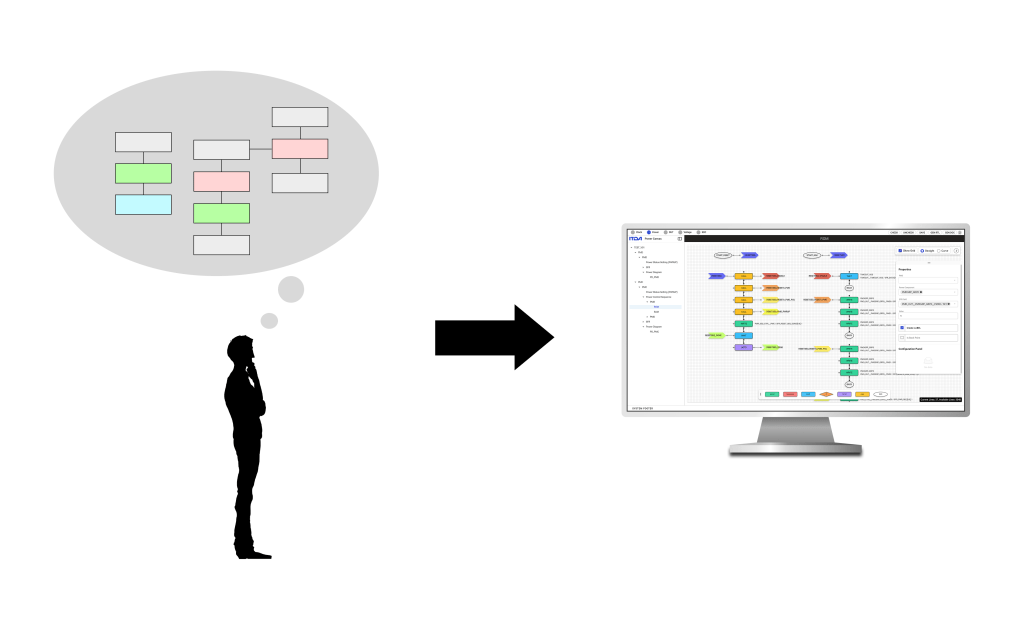
In their minds, they see an array of boxes—sometimes dozens of them—representing processing units or functional blocks.
Design meetings often end with hundreds of drawn boxes, without progressing beyond that.
In other words, designers view a chip as a collection of meaningful units or processing structures.
Yet there is no standardized way to illustrate these ideas.
As a result, semiconductor architects often spend more time using tools like Visio or draw.io to draw diagrams than they do coding.
That’s why we believe semiconductor design should be done through a GUI: to express the designers’ thoughts directly.
A GUI allows design to be done in a standardized way that all designers can understand, not just as a collection of boxes.
Of course, not all design can be done purely through a GUI. GUIs are most suitable for repetitive and standardized structures, and it is difficult to reflect newly evolving processing units or algorithms.
However, just as cities may have different buildings but similar infrastructure—roads, electricity, water—semiconductor design infrastructure is largely similar across projects.
If the infrastructure is comparable, we believed GUI-based design is feasible.
And that is how SOC Canvas was born.
Power Canvas allows a Power System designer to complete a design simply by drawing flowchart-style diagrams, familiar to anyone in that field.
Clock Canvas allows a Clock System designer to complete a design by drawing a Clock Tree, a concept familiar to all clock engineers.
In other words, to align the level of understanding with the level of design, a GUI is essential.
A GUI is not just a technology.
It is a new design language that implements exactly what the designer imagines and makes it accessible to anyone.
That is why SoC Canvas was created with an intuitive interface, a GUI that anyone can understand, to deliver unparalleled convenience to designers.
왜 제품을 GUI로 만들어야 했을까요?
GUI는 Graphic User Interface 즉, 사용자가 그림으로 조작하도록 만든 인터페이스입니다.
조금 다르게 표현해보자면, 소통하는 방식이 그림이라는 얘기입니다.
언어도, 글도 소통의 방식이긴 하지만 배우고 익혀야 합니다. 근데, 그림은 다릅니다. 배우지 않아도 직관적으로 이해할 수 있죠.
보이는 모습 그대로 표현되기 때문에 언어와 문화가 달라도 누구나 보는 순간 의미를 알 수 있습니다. 게다가 클릭이나 스크롤같은 단순한 행동으로 원하는 바를 바로 실행할 수 있습니다.
GUI는 인간의 감각과 사고 구조에 맞춘 가장 자연스러운, 그래서 가장 직관적인 소통방식입니다.
그렇기 때문에 맥킨토시에 GUI가 적용되고 나서,
컴퓨터는 더이상 fortran이나 c언어를 아는 전문가들만의 도구가 아닌,
일상에서 누구나 사용할 수 있는 도구가 될 수가 있었던 겁니다.
그래서 우리 제품도 GUI로 만들었습니다.
반도체 엔지니어들의 생각을 그대로 표현하고, 설계를 더 쉽게 하기 위해서.
반도체 설계는 verilog나 c언어로 코딩하지만, 대부분의 설계자들은 반도체를 verilog나 c로 이해하지 않습니다.
설계자들의 머릿속에는 네모박스들만 엄청나게 들어가 있죠. 만나서 설계회의를 해보면, 박스들만 수십개 그리다 끝나는 경우가 많습니다.
즉, 설계자들은 설계를 의미있는 정보들의 집합 혹은 프로세싱 유닛으로 보고 있다는 말입니다.
근데, 이를 설명하기 위한 그림은 정형화된 방법이 없습니다.
그래서 반도체 아키텍트들은 visio나 draw.io를 사용하는 시간이 코딩하는 시간보다 훨씬 길거에요.
그렇기 때문에, GUI로 설계를 해야 된다고 생각합니다.
설계자들의 생각을 그대로 표현해야하기 때문이죠.
GUI는 네모박스가 아닌, 모든 설계자들이 이해할 수 있는 정형화된 방법으로 설계할 수 있게 해줍니다.
물론 모든 설계를 GUI로만 할 수는 없습니다. GUI는 반복적이고 정형화된 구조에 적합하기 때문에, 매번 업데이트 되고 새롭게 바뀌는 프로세싱 유닛이나 알고리즘은 반영하기 어렵습니다.
하지만, 도시의 빌딩들은 다 달라도, 수도,전기,도로 같은 인프라는 비슷한 것처럼 반도체 설계의 인프라도 크게 다르지 않다면,
GUI로 할만하다고 생각했고,
그렇게 해서 SOC Canvas가 만들어졌습니다.
Power Canvas는 Power System 설계자라면 누구나 생각하는 플로우 차트 형태로 그림을 그리면 설계가 완성됩니다.
Clock Canvas는 Clock System 설계자라면 누구나 이해하는 Clock Tree 를 그리면 설계가 완성됩니다.
즉, 이해의 레벨과 설계의 레벨을 완전히 동일하게 하기 위해서는 GUI가 필수였습니다.
GUI는 단순한 기술이 아닙니다.
설계자가 생각하는 것을 그대로 구현해주고, 누구나 사용할 수 있는 새로운 설계 언어입니다.
그래서 SoC Canvas는 설계자들의 압도적 편의성을 위해 누구나 이해할 수 있는 직관적인 인터페이스, GUI로 만들어졌습니다.