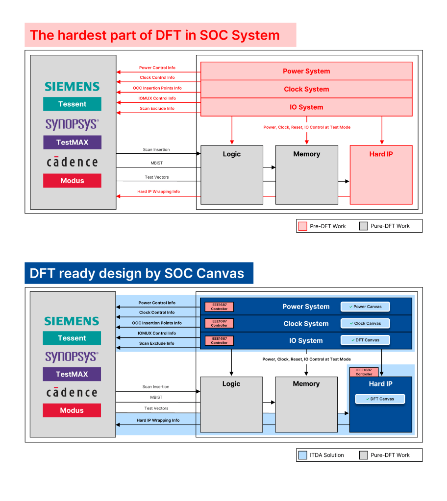
Looking at the difficulties of DFT organized so far, they were not difficulties with DFT itself, but difficulties with building infrastructure for DFT insertion.
This means that if the infrastructure is built, DFT can be inserted right away.
There are two things to consider when building infrastructure for DFT insertion.
1. Information transmission
– PIN information for power control
– PIN information for clock control
– OCC (On Chip Controller) insertion point
– Table for I/O configuration
– List of Flip-Flops that should not be linked to SCAN
2. Design preparation
– Design of Power, Clock, I/O System controllable in IEEE1687 or test mode
– Separate System configuration for Hard IP test controllable in IEEE1687 or test mode
The design targets for this infrastructure were Power, Clock, and I/O System, and the System for testing Hard IP must be prepared as a separate solution.
SoC Canvas builds an infrastructure for DFT insertion that considers all of this through Power Canvas, Clock Canvas, and DFT Canvas.
1. Power Canvas
– Transferring PIN information for power control and generating vectors
– Designing a power system that can be controlled in IEEE1687 or test mode
– Managing the list of Flip-Flops that must not be linked to SCAN
2. Clock Canvas
– Transferring PIN information for clock control and generating vectors
– Transferring point information for inserting OCC (On Chip Controller)
– Designing a clock system that can be controlled in IEEE1687 or test mode
– Managing the list of Flip-Flops that must not be linked to SCAN
3. DFT Canvas
– Transferring IOMUX control information
– Designing an I/O that can be controlled in IEEE1687 or test mode
– Mapping Hard IP PIN information to I/O information
– Managing the list of structures that must not be linked to SCAN
With these three solutions, you can complete the functional design and prepare for DFT insertion at the same time.
Compared to the current design method that analyzes the structure in the functional mode, analyzes the DFT separately, and then inserts the DFT,
it is possible to shorten the design time by up to 3 to 6 months. This is closely related to enhancing the competitiveness of the chip and reducing design costs.
The shorter the design period, the more cutting-edge ideas can be reflected, and the faster they can be put on the market, which increases the competitiveness of the chip.
If the overall design period of the chip can be reduced, the labor cost and design cost will decrease proportionally. During DFT insertion, the design personnel cannot proceed with the design because they have to check the parts that change according to DFT, even if they do not proceed with the design.
In this respect, SOC Canvas can raise the competitiveness of the chip to the next level.
지금까지 정리한 DFT의 어려움들을 보면 다 DFT자체의 어려움이 아니라, DFT insertion을 위한 인프라를 구축하는 어려움이었습니다.
인프라가 구축되어 있다면, 바로 DFT를 삽입할 수 있다는 얘기입니다.
DFT insertion을 위한 인프라를 구축할 때 고려해야 할 사항은 2가지 입니다.
1. 정보 전달
– Power 제어를 위한 PIN 정보
– Clock 제어를 위한 PIN 정보
– OCC (On Chip Controller) 삽입 포인트
– I/O 구성에 대한 테이블
– SCAN을 엮지 않아야 하는 Flip-Flop의 리스트
2. 설계 준비
– IEEE1687 혹은 테스트 모드에서 제어 가능한 Power, Clock, I/O System 설계
– IEEE1687 혹은 테스트 모드에서 제어 가능한 Hard IP 테스트를 위한 별도 System 구성
이러한 인프라에 해당하는 설계 대상은 Power, Clock, I/O System이었고, Hard IP를 테스트 하기 위한 System은 별도의 솔루션으로 준비가 되어야 합니다.
SoC Canvas는 Power Canvas, Clock Canvas, DFT Canvas를 통해, 이를 모두 고려한 DFT insertion을 위한 인프라를 구축합니다.
1. Power Canvas
Power 제어를 위한 PIN 정보 전달 및 vector 생성
IEEE1687 혹은 테스트 모드에서 제어 가능한 Power System 설계
SCAN을 엮지 않아야 하는 Flip-Flop의 리스트 관리
2. Clock Canvas
Clock 제어를 위한 PIN 정보 전달 및 vector 생성
OCC (On Chip Controller) 삽입을 위한 포인트 정보 전달
IEEE1687 혹은 테스트 모드에서 제어 가능한 Clock System설계
SCAN을 엮지 않아야 하는 Flip-Flop의 리스트 관리
3. DFT Canvas
IOMUX control 정보 전달
IEEE1687 혹은 테스트 모드에서 제어 가능한 I/O설계
Hard IP PIN 정보를 I/O 정보에 mapping
SCAN을 엮지 않아야 하는 구조 리스트 관리
3개의 솔루션을 통해, 기능 설계를 끝냄과 동시에, DFT insertion에 대한 준비도 모두 마칠 수 있게 됩니다.
기능 모드의 구조를 분석하고 DFT를 별도로 분석해서 DFT를 insertion하는 현재의 설계 방식과 비교하면,
최대 3~6개월 이상의 설계 시간 단축이 가능합니다. 이는 곧 칩의 경쟁력 강화와 설계 비용 감축과 밀접한 관계가 있습니다.
설계 기간이 짧을 수록 더 많은 최신 아이디어를 반영할 수 있고, 시장에 더 빨리 내놓을 수 있으니, 칩의 경쟁력이 더 올라갑니다.
칩의 전체 설계 기간을 줄일 수 있다면, 인건비와 설계 비용은 그 비율대로 내려갑니다. DFT insertion 하는 동안 설계 인력은 설계를 진행하지 않더라도, DFT에 따라 변경되는 부분을 확인해야 하니 다른 칩의 설계를 진행할 수는 없기 때문입니다.
SOC canvas는 이런 측면에서, 칩의 경쟁력을 한 차원 끌어올릴 수 있습니다.